


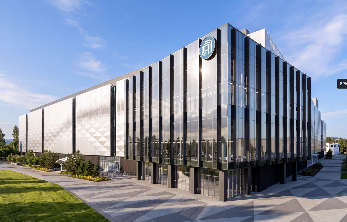
Applied Materials has opened a new $5 billion semiconductor research facility in Silicon Valley focused on accelerating innovation in chip manufacturing. The company says the site is its Equipment and Process Innovation and Commercialization (EPIC) Center, designed to support collaborative work aimed at advancing the next generation of commercially produced chips.
According to coverage of the launch, the center brings together Applied teams with researchers and engineers from companies and universities, with the goal of speeding development cycles for semiconductor processes and equipment. Outlets also frame the initiative as part of the broader push to streamline AI-related chipmaking, reflecting demand for improved manufacturing approaches as AI workloads drive new chip requirements.
While both reports emphasize collaboration and faster breakthroughs, they differ slightly in emphasis: one highlights the scale and role of the center in enabling “the next wave” of chipmaking breakthroughs, while the other foregrounds AI manufacturing efficiency. Both describe Applied Materials as a major supplier used by major chipmakers, including TSMC, Intel and Samsung.


